The MIPS8 Processor was developed for my Integrated Circuits Design course at
John Brown University. It implements an 8-bit MIPS-style processor in Electric VLSI.
The project followed a complete custom IC design flow, including transistor-level
schematics, physical layout design, verification, and functional simulation.
Major components such as the datapath, ALU, control logic, and padframe
integration were implemented and validated throughout the design process.
Verification was performed using DRC, ERC, NCC, and switch-level simulation to
ensure both physical correctness and functional behavior. Test programs and
assertion-based command files were used to confirm correct execution of MIPS8
instructions.
The main challenge was not only making the logic work, but also translating the
architecture into a physical IC layout that passes verification.
How It Works
Engineering notes.
Building a processor below the HDL level requires more than describing
behavior in Verilog or testing an architecture in software. The logic
must be constructed from smaller cells, connected through schematics,
translated into layout, and checked as a physical design.
The goal was to implement an 8-bit MIPS-style processor while keeping
the schematic hierarchy, layout, and functional behavior consistent
throughout the custom IC flow.
Instructions move through a simple MIPS-style datapath. The datapath
connects the program counter, instruction decoding, register file, ALU,
control logic, and memory-related signals. The ALU performs arithmetic
and logic operations, while the control logic selects the correct path
for each instruction.
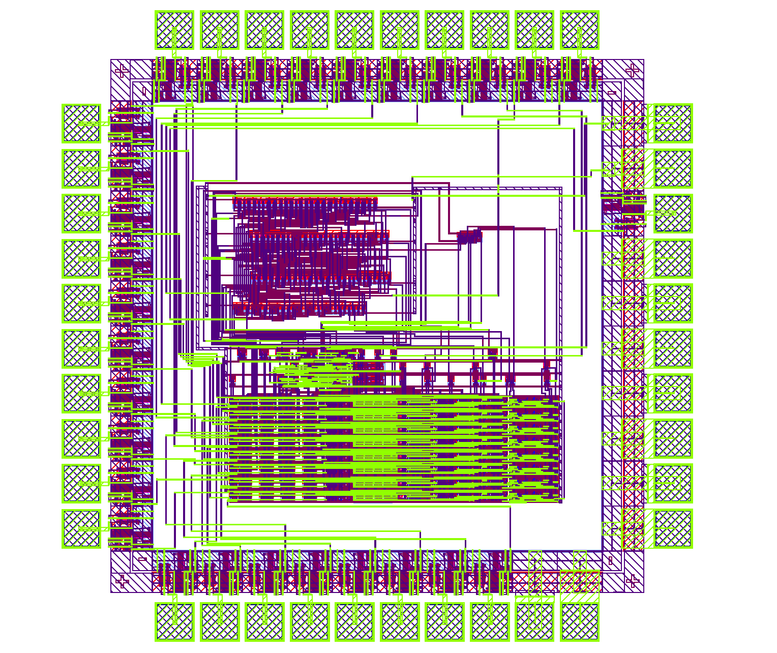
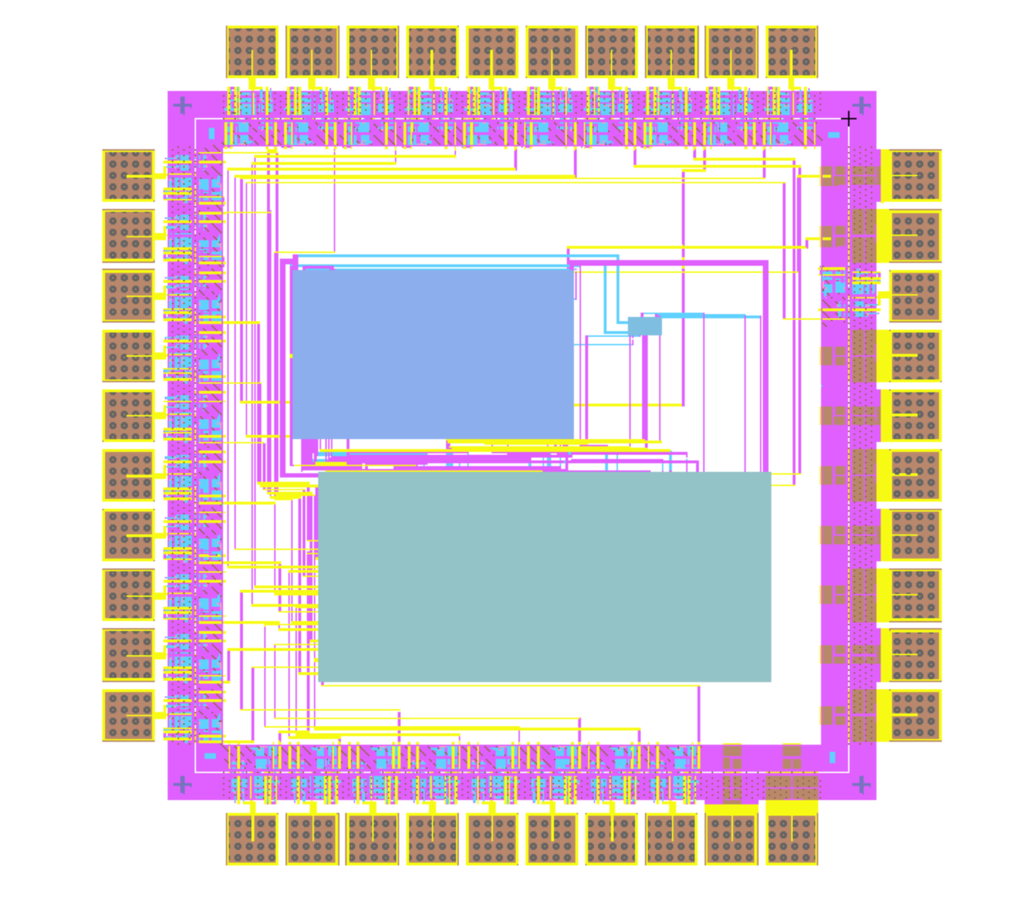
The design follows a hierarchy: smaller verified cells build larger
blocks, and those blocks connect at the processor level. The final
integration includes the processor core and the top-level padframe.
The project followed a custom IC design flow in Electric VLSI:
Design and verify transistor-level cells.
Build larger schematic blocks from verified cells.
Connect the processor datapath and control logic.
Create physical layouts for cells and major blocks.
Run DRC, ERC, and NCC checks.
Simulate behavior with IRSIM and command files.
Integrate the completed design with the top-level padframe.
The physical implementation required careful routing and hierarchy
management so each layout block remained consistent with its schematic.
Verification covered both physical correctness and functional behavior.
DRC checked layout design rules, ERC checked electrical connection
problems, and NCC confirmed that each schematic matched its layout.
IRSIM switch-level simulation tested processor behavior during
instruction execution. Test programs and assertion-based .cmd files
checked expected outputs, register writes, and program counter changes.
The final processor was completed and successfully verified at the
schematic and layout level. The completed design connects the datapath,
ALU, control logic, and padframe through a consistent hierarchy.
The project showed the full path from a digital processor architecture
to a physical IC implementation, including layout, verification, and
switch-level simulation.
Interactive Demo
MIPS8 instruction stepper.
A simplified instruction-level demo inspired by the processor. Step through a
short program to see how data moves across the datapath.